From our front-page news:
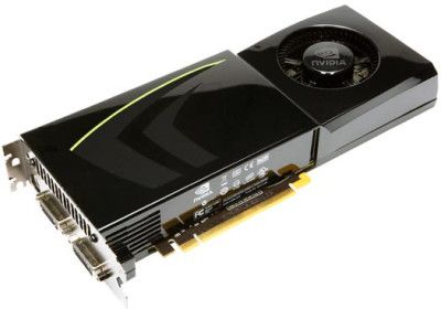
NVIDIA hasn't been having the best of news to pass around lately, and it sure doesn't look like that run is going to end anytime soon. New reports out of the Electronic Thin Film lab of the Department of Materials Science and Engineering at the University of California at Los Angeles (seriously!) show that NVIDIA's choice of using a solder with high-lead will suffer the fate of cracking under high temperatures (70°C+), whereas eutectic solder, used by ATI, will last much longer.
At first glance, this doesn't seem to be a large issue, but it looks like the reason NVIDIA's had issues with their mobile GPUs might be due to this solder, and what a mistake to make. To date, it's supposedly cost the company over $200 million to deal with, so changes definitely need to be made.
The problem now is that we need to wait to see a change happen, since it's not as simple as simply switching out the solder used. It requires certain changes to be made to the power delivery, and it goes without saying, anything like that is going to take more than a few weeks to thoroughly test. There's also the question of whether or not the current GPUs on the market are actually going to break down due to this solder, especially desktop cards.
Overall, Tu believes that the high-lead solder joint "has a built-in weakness" due to the thin layer of eutectic SnPb solder in the joint. "The eutectic SnPb has a low yield stress and it will deform first and lead to stress concentration and to accumulate high plastic strain energy," Tu writes. In contrast, the "homogeneous eutectic SnPb solder joint tends to have a uniform composition and much lower plastic deformation so the accumulation of plastic strain energy per unit volume is lower."
Source: TG Daily