TSMC Begins Volume Production of 28nm Parts

Rob Williams

Editor-in-Chief
Staff member
Moderator
TSMC, the Taiwanese semiconductor company responsible for producing silicon for both of the leading discrete GPU manufacturers, has just announced that it has begun volume production of wafers built on a 28nm process. Of these, four variants exist; High Performance, High Performance Low Power, Low Power and High Performance Mobile Computing - the latter being a bit special in that it won't actually become available until next year.
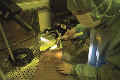
tsmc_102611.jpg

Read the rest of our post and then discuss it here!
 

marfig

No ROM battery
An impressive move. From 40nm to 28nm in just one generation. Couldn't this make the current generation of GPUS very rapidly obsolete, at least in terms of power consumption?

A couple of months ago I was reading somewhere else how cards like the GTX 560 Ti could become a standard for the next ~2 years. But I'm just not so sure anymore.
 

Kougar

Techgage Staff
Staff member
Whatever envelope saved in power consumption will just be re-used for additional silicon or higher clockspeeds, sometimes both. Can't say for sure until the new stuff comes out! Given AMD gave up the pursuit of "bigger is better", they are the more likely candidate to reflect power savings in their parts though...

Speaking of the new stuff, Nvidia's Kepler is using this 28nm process, and is expected to debut early spring, delayed from a Thanksgiving launch. Given it has 3x the double-precision performance, I am quite eager to see how its single-precision performance compares to Fermi.
 
Top